News from October 2026
665 stories of semiconductor news published on the Hub in October 2026, newest first and grouped by day (UTC). Each headline opens the story's page on the Hub, with a summary and a link to the original report.
Showing 601 to 650 of 665 stories.
Friday 23 October 202695 stories
Beyond The EPE Budget: Building The Next Generation Of Computational LithographyEDA & Tools · Semiconductor Engineering · Summary

Image: Semiconductor Engineering (opens in a new tab) Why better models, richer metrology, explainable AI, and cross-industry collaboration must come together to extend semiconductor scaling. The post Beyond The EPE Budget: Building The Next Generation Of Computational Lithography appeared first on Semiconductor Engineering.
Everspin Expands MRAM Push into AI Servers, Data Centers, Satellite SystemsDesign & IP · EE Times · Summary

Image: EE Times (opens in a new tab) In an exclusive interview, Everspin CEO Sanjeev Aggarwal discusses MRAM opportunities amid NOR flash supply constraints. The post Everspin Expands MRAM Push into AI Servers, Data Centers, Satellite Systems appeared first on EE Times.
How Goodram Validates DRAM and SSD Reliability in EuropePackaging & Test · EE Times · Summary

Image: EE Times (opens in a new tab) Explore Goodram’s European approach to DRAM and SSD testing, from burn-in to platform validation, for reliable industrial and embedded systems. The post How Goodram Validates DRAM and SSD Reliability in Europe appeared first on EE Times.
Deepx Building Open Software Ecosystem to Scale Physical AI Beyond the Data CenterDesign & IP · EE Times · Summary

Image: EE Times (opens in a new tab) Deepx is combining low-power AI accelerators and portable software with industry partnerships to bring physical AI into production. The post Deepx Building Open Software Ecosystem to Scale Physical AI Beyond the Data Center appeared first on EE Times.
From Cloud AI to Edge AI: How BIWIN Enables the Next Generation of Storage and Memory SolutionsDesign & IP · EE Times · Summary

Image: EE Times (opens in a new tab) See how BIWIN’s SSD, embedded storage, and memory portfolio supports faster, efficient AI from cloud data centers to edge wearables. The post From Cloud AI to Edge AI: How BIWIN Enables the Next Generation of Storage and Memory Solutions appeared first on EE Times.
Data Center Power Cable Market to Reach USD 4.72 Billion by 2035 as AI Campuses Pull Medium-Voltage Distribution Deeper Into the Data Hall - DC Market InsightsMarkets & Policy · PR Newswire · Summary
Market grows at a 10.50% CAGR from USD 1.74 billion in 2025; low-voltage power cables hold 40.4% of spending, DC power cables grow fastest at 11.55% a year and North America leads with 42.0% LONDON, Oct. 22, 2026 /PRNewswire/ -- The 'Data Center Power Cable Market - Growth, Share,...
UMC and AP Memory Collaborate to Enable Advanced Power Delivery Solutions for AI and HPC SystemsFoundry & Manufacturing · PR Newswire · Summary
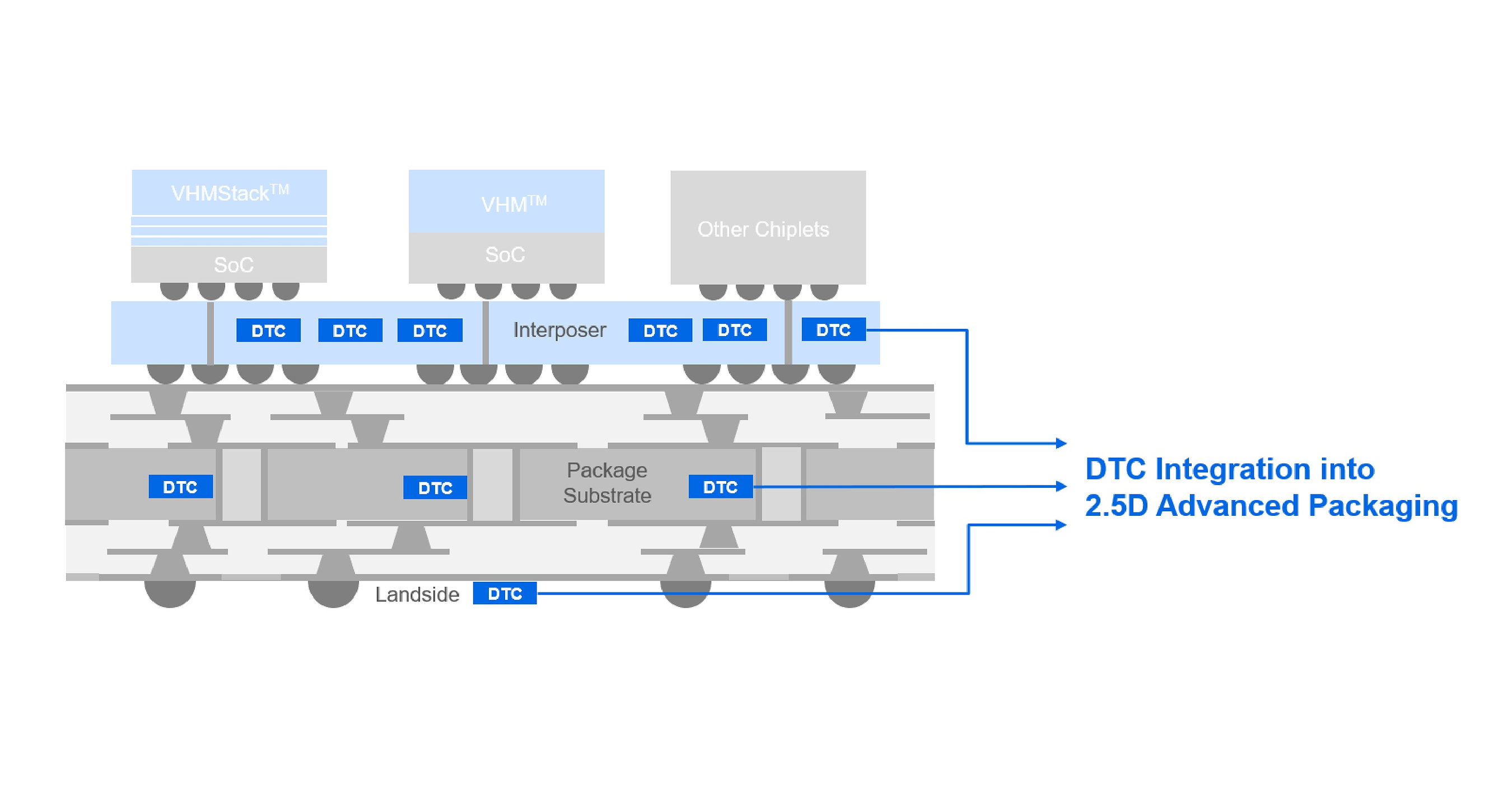
Image: PR Newswire (opens in a new tab) HSINCHU, Oct. 22, 2026 /PRNewswire/ -- United Microelectronics Corporation (NYSE: UMC; TWSE: 2303) ("UMC") and AP Memory (TWSE: 6531) today announced a technology and manufacturing collaboration to advance power delivery solutions for AI and high-performance computing (HPC) systems. This...
Innoviz Sets Third Quarter 2026 Conference Call for Wednesday, November 11 at 9:00 a.m. ETMarkets & Policy · PR Newswire · Summary
TEL AVIV, Israel, Oct. 22, 2026 /PRNewswire/ -- Innoviz Technologies Ltd. (NASDAQ: INVZ) (the "Company" or "Innoviz"), a leading supplier of high-performance, automotive-grade LiDAR sensor platforms for autonomous driving, defense and homeland security, industrial, and smart...
LG Innotek is Collaborating with NVIDIA, Taking One Step Closer to Securing a Leading Position in the Physical AI MarketMarkets & Policy · PR Newswire · Summary
Showcases NVIDIA-focused solutions, including camera modules and a Multi-modal Vision System, at GTC Berlin on October 20 Collaboration to expand into robotic vision sensing and robotic hands; next-generation solutions to be unveiled next year Accelerating leadership in the Physical AI...
Building Out Advanced Packaging Portfolio, JCET Delivers Steady Revenue Growth and Improved Profitability in Q3 YTD 2026Packaging & Test · PR Newswire · Summary
SHANGHAI, Oct. 22, 2026 /PRNewswire/ -- Today, JCET Group (SSE: 600584), a leading global provider of integrated circuit (IC) back-end manufacturing and technology services, released its financial results for the third quarter of 2026. For the first nine months of 2026, JCET recorded...
LattePanda Launches LattePanda Sigma 2: The Embeddable AI Single Board ServerDesign & IP · PR Newswire · Summary
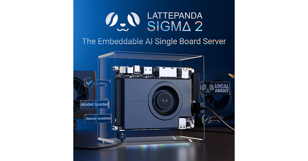
Image: PR Newswire (opens in a new tab) SHANGHAI, Oct. 22, 2026 /PRNewswire/ -- The LattePanda Team today launched LattePanda Sigma 2, an x86 single-board server designed to bring high-performance local AI computing directly into intelligent products and systems. Built around the Intel® Core™ Ultra X7 358H processor with Intel...
Spectrum Control Earns Platinum Award in 2026 Military + Aerospace Electronics Innovators AwardDesign & IP · PR Newswire · Summary
FAIRVIEW, Pa., Oct. 22, 2026 /PRNewswire/ -- Spectrum Control, a leader in RF miniaturization and RF+Digital™ integration, announces its 16-channel DirectRF+™ Wideband Direct Sampling Transceiver in 3U VPX was recognized among the best technology solutions by the 2026 MAE Innovators...
Analog Devices to Report Fourth Quarter Fiscal Year 2026 Financial Results on Tuesday, November 24, 2026Markets & Policy · PR Newswire · Summary
WILMINGTON, Mass., Oct. 22, 2026 /PRNewswire/ -- Analog Devices, Inc. (Nasdaq: ADI) today announced it will release financial results for the fourth quarter fiscal year 2026 at 7:00 a.m. Eastern time on Tuesday, November 24, 2026. Following the press release, the Company will host a...
Quantinuum to Report Third Quarter Financial Results on November 5, 2026Markets & Policy · PR Newswire · Summary
BROOMFIELD, Colo., Oct. 22, 2026 /PRNewswire/ -- Quantinuum Inc. (NASDAQ: QNT) ("Quantinuum") today announced it will release its financial results for the third quarter ended September 30, 2026, on November 5, 2026, after market close. Quantinuum will host a conference call at 5:00 PM...
Bulletin from Sivers Semiconductors AB's Extraordinary General Meeting on 22 October 2026Markets & Policy · PR Newswire · Summary
KISTA, Sweden, Oct. 22, 2026 /PRNewswire/ -- The Extraordinary General Meeting in Sivers Semiconductors AB (the "Company") was held on 22 October 2026 and in particular the following resolutions were resolved. Election of auditor The Extraordinary General Meeting resolved, in accordance...
How AI infrastructure will be designed for the futureDesign & IP · SK hynix · Summary
AI is no longer defined by a single model or AI processor. For AI to operate effectively in real-world services and industrial applications, it takes faster compute, wider memory bandwidth, higher-performance networks, more efficient storage, and more stable power and
Solidigm to Discontinue Review of Potential IPO, Reaffirming Commitment to Long-Term Growth and Shareholder ValueMarkets & Policy · SK hynix · Summary
▪ Solidigm has explored various funding options, including a potential IPO, to finance a new fab in the U.S. to meet growing AI memory demand. ▪ While an IPO was expected to ease investment burdens and expand capacity for shareholder
How Companies Are Using NVIDIA DSX to Break the Power BottleneckMarkets & Policy · NVIDIA · Summary

Image: NVIDIA (opens in a new tab) Companies around the world are building on the NVIDIA DSX AI Factory Platform to plan, simulate and run the grid and the AI factory as one system, from the substation to the rack. Their adoption of the platform responds to an acute problem.
Power is now the biggest bottleneck in infrastructure. More than $300 billion […]
NVIDIA Unveils Minerva to Bring End-to-End Observability for AI FactoriesMarkets & Policy · NVIDIA · Summary
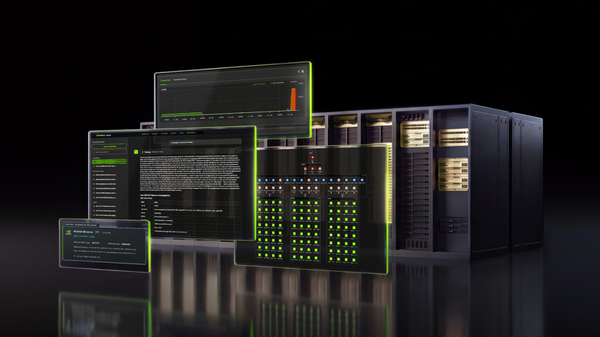
Image: NVIDIA (opens in a new tab) Launched today, NVIDIA Minerva is an AIOps platform built to help teams find problems earlier and keep AI factories productive. It brings together telemetry from infrastructure and AI workloads, then applies purpose-built AI models to turn that data into timely, actionable insight.
AI factories are among the most complex operations in the world, with vast […]
Qualcomm Schedules Fourth Quarter and Fiscal 2026 Earnings Release and Conference CallMarkets & Policy · Qualcomm · Summary
// // SAN DIEGO, Oct. 22, 2026 /PRNewswire/ -- Qualcomm Incorporated (NASDAQ: QCOM) today announced that it will publish the Company's financial results for its fo…
Intel hits construction milestone at Ohio chip fab that’s at least 5 years behind scheduleFoundry & Manufacturing · CNBC Technology · Summary

Image: CNBC Technology (opens in a new tab) Intel has installed the first major structural truss at its delayed Ohio chip fab, but the company has yet to announce a major outside customer.
Rambus adopts ChipAgents across its design teams and invests in the companyEDA & Tools · Rambus · Summary

Image: Rambus (opens in a new tab) Rambus is rolling out the ChipAgents agentic AI platform across its chip and silicon IP design and verification work, and has made a strategic investment in the company, with terms not disclosed.
ChipAgents, founded in 2024 and based in Santa Clara, California, makes AI agents that turn specifications and code into RTL, verification assets and automated root-cause analysis. The two companies also plan to support customers' design work in their own design environments.
Wednesday 21 October 202641 stories
US think tank report calls for a China wide ban on DUV immersion exportsMarkets & Policy · Bits&Chips · Summary
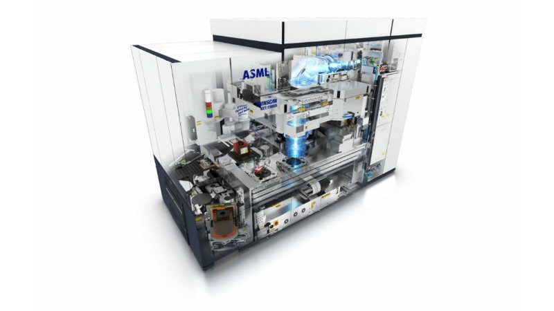
Image: Bits&Chips (opens in a new tab) The Center for Technology and Statecraft, a US think tank backed by the Institute for Progress, has published a report urging a ban on exports of DUV immersion lithography systems to all of China, together with tighter limits on servicing and spare parts. Dry DUV tools used for less advanced chips would remain available.
The authors are Nicholas Brown, formerly a senior policy adviser at the Commerce Department's Bureau of Industry and Security, and Saif Khan, formerly director for technology and national security at the National Security Council. Such a ban would mainly affect ASML in the Netherlands and Nikon in Japan.
The report estimates that Chinese owned fabs had accumulated more than 330 immersion systems by early 2026 and argues that continued imports, if directed at AI chips, could bring Chinese output close to or above that of the United States and its allies.
It follows the proposed Match Act in Congress, which would impose similar limits, and US warnings of unilateral action if allies do not align.
Chinese start up Langdao Silex shows a 15 watt EUV light source prototypeEquipment & Materials · Bits&Chips · Summary
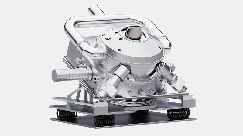
Image: Bits&Chips (opens in a new tab) Langdao Silex, a Chinese start up founded in 2024 by alumni of Tsinghua University's gas discharge plasma laboratory, has presented a prototype extreme ultraviolet light source at an exhibition in Shanghai. Like ASML's sources, it uses laser produced plasma, and the company says 90 per cent of its components come from domestic suppliers.
It claims output above 15 watts and continuous operation for more than 100 hours, but the source was not shown running and the company has not said where in the optical path the power is measured.
That makes a direct comparison with ASML difficult, because ASML quotes usable power at the intermediate focus after collection losses; its first source for volume manufacturing delivered 250 watts.
Bits&Chips concludes that the prototype could support research on EUV resists, optics and experimental exposures, but is far too weak for commercial chip production. Langdao is reported to be working on a higher power version and expects commercial use in three to five years.
Fortior agrees to buy Eindhoven sensor chip designer SciosenseDesign & IP · Bits&Chips · Summary
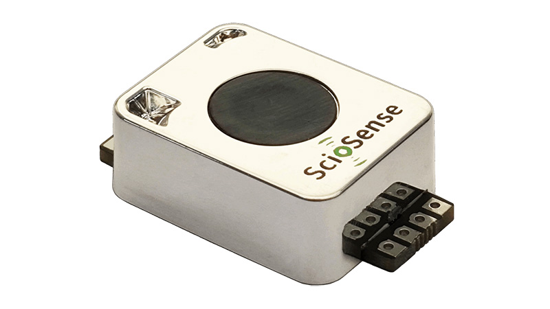
Image: Bits&Chips (opens in a new tab) Fortior, a Chinese maker of motor control chips, plans to acquire Sciosense, a sensor chip designer headquartered in Eindhoven, in a deal worth up to US$118 million.
Sciosense is currently owned 51 per cent by the Chinese investment firm Wise Road Capital and 49 per cent by the Austrian company ams OSRAM, which formed it in 2019 as a joint venture around ams's environmental, flow and pressure sensor business.
The company's portfolio also includes businesses acquired earlier, among them Appliedsensor and acam messelectronic, NXP's advanced CMOS sensor activities and Cambridge CMOS Sensors.
Sciosense has been under majority Chinese ownership for several years, but Bits&Chips notes that the timing is sensitive because relations between the Netherlands and China are only now recovering from the dispute over Nexperia.
The European Union is also working to narrow its trade deficit with China and is screening foreign direct investment in strategic industries. Approval requirements and an expected closing date were not reported.
Besi joins Applied's EPIC Center to extend hybrid bonding workPackaging & Test · Bits&Chips · Summary
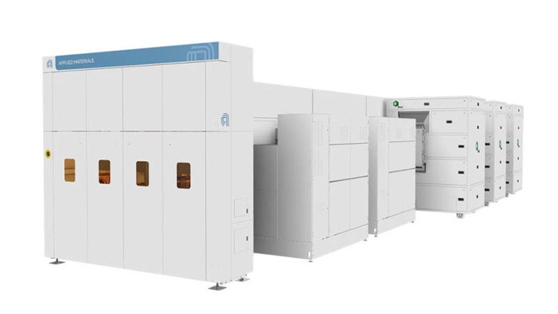
Image: Bits&Chips (opens in a new tab) Besi, the Dutch assembly equipment maker, is joining Applied Materials' EPIC Center in Silicon Valley as an innovation partner, with Besi engineers working alongside Applied's teams.
The partnership, which so far has concentrated on die to wafer hybrid bonding, now extends to the next steps in 3D integration and to combining logic and memory. Planned research covers die on wafer, die on die and die on panel integration, as well as interconnects that use photonics.
The two companies started working together in 2020 at a joint hybrid bonding centre in Singapore, which produced Kinex, a die to wafer bonding system that combines Applied's wafer processing with Besi's die placement and assembly.
Hybrid bonding joins copper pads directly without solder bumps, allowing much finer connection pitches for stacked chips and chiplets.
Applied expects the EPIC Center to be operating this year and its capital spending to build towards about US$5 billion over time, bringing suppliers and chipmakers together to shorten the path from research to production.
IBM and Siemens to model IBM's stacked nanosheet transistor architectureEDA & Tools · eeNews Europe · Summary

Image: eeNews Europe (opens in a new tab) IBM and Siemens have agreed a research collaboration on IBM's nanostack transistor architecture, which IBM unveiled earlier in 2026 as a candidate for chips at angstrom scale.
Nanostack stacks staggered nanosheet transistors vertically to raise density, performance and energy efficiency, and IBM says it can fit close to 100 billion transistors in an area the size of a fingernail at its current 7 angstrom node.
Different semiconductor materials can be used in individual layers of the stack, so the power and performance of each transistor can be tuned separately. Siemens brings electronic design automation, simulation and lithography expertise.
Together the companies will build virtual models to predict transistor behaviour, optimise designs and catch manufacturing problems before anything is fabricated, with the work planned to continue beyond the 7 angstrom generation. IBM describes nanostack as moving device scaling from two dimensions to three.
No production timeline has been announced, and no foundry partner for manufacturing has been named.
Yole sees data centre CPUs and networking chips gaining on GPUsMarkets & Policy · Electronics Weekly · Summary

Image: Electronics Weekly (opens in a new tab) Yole Group's data centre processor tracking, reported by Electronics Weekly, shows data centre CPU revenue of about US$13.2 billion in the second quarter of 2026, growing around 35 per cent on the previous quarter as agentic AI workloads add demand for general purpose compute.
That outpaced AI ASICs, up 23 per cent to US$15.1 billion, and GPUs, up 13 per cent to US$66.3 billion. Yole also reports that some GPU and ASIC designers are trimming their roadmaps because of steep DRAM price rises.
Networking is the fastest growing data centre chip segment in its forecasts: worth about US$53 billion in 2026, it is expected to rise from about 13 to 34 per cent of the data centre semiconductor market by 2031.
Scale up switch revenue is forecast to grow 59 per cent a year to US$42 billion by 2031, with co packaged optics making up 23 per cent of that. Broadcom leads scale out switching, with Nvidia close behind and leading network interface cards.
E&R opens a Malaysian plant for semiconductor carrier tapePackaging & Test · Evertiq · Summary
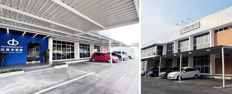
Image: Evertiq (opens in a new tab) E&R Engineering, a Taiwanese maker of semiconductor packaging equipment, has opened a Malaysian subsidiary, E&R Semiconductor (Malaysia), to produce packaging materials closer to customers in Southeast Asia. The plant is in sample testing and qualification, and mass production is planned for early next year.
It is expected to create about 50 local jobs and will also serve as a base for the company's equipment and field service engineers in the region.
E&R says the site will give semiconductor makers and outsourced assembly and test customers faster technical support and more flexible supply, as part of a broader shift of some production to Malaysia while it expands capacity.
Company president KS Chen called the opening a milestone in the international growth of its carrier tape business, the reeled tape used to hold and feed packaged chips during assembly. The plant's general manager, AK Ong, said being closer to customers is the main benefit and stressed strict quality checks.
Investment figures were not given.
Neways to package Melexis Triphibian pressure sensors under a multi year dealPackaging & Test · Evertiq · Summary

Image: Evertiq (opens in a new tab) Neways Electronics has signed a multi year agreement with Melexis to package the Belgian company's Triphibian pressure sensors. These MEMS devices measure pressure in both liquids and gases and are used in thermal management systems for electric vehicles and for liquid cooled AI data centres.
According to Neways, the package that protects the sensor die has a strong influence on accuracy, durability and the cost of producing the sensor in volume, so engineers from both companies worked together on a compact package designed for harsh operating conditions.
Neways chief executive Hans Büthker said advanced packaging is a strategic focus for the group as it builds a packaging business for semiconductor and sensor makers. Melexis chief executive Marc Biron said Melexis chose Neways as its development partner because of its packaging expertise in the early design phase.
Neways adds that the same package could suit other compact pressure sensing uses. The value, length and volumes of the deal were not disclosed.
MintNeuro raises $5 million for chips aimed at neural implants and wearablesDesign & IP · Evertiq · Summary

Image: Evertiq (opens in a new tab) MintNeuro, a London based semiconductor start up that designs chips for neurotechnology products such as implants and wearables, has closed a US$5 million funding round. Odyssey Ventures led the round, with 33East, JSK Investments and Alumni Ventures joining and Empirical Ventures, Jumpspace Ventures and earlier backers investing again.
The company's pitch is that its chips perform better than generic components while costing less, carrying less risk and reaching market faster than a device maker designing its own custom silicon.
The money will go on larger engineering and sales teams, product launches, support for customers integrating its chips and expansion into the United States from its base in the United Kingdom and Europe.
Chief executive Dorian Haci described the round as the move from proving the technology to scaling it commercially, and the company's chair, Tim Denison, said specialised hardware will be central to the growth of the neurotechnology field. Terms beyond the amount raised were not published.
Ubitium raises $14 million for a single processor for autonomous machinesDesign & IP · Evertiq · Summary
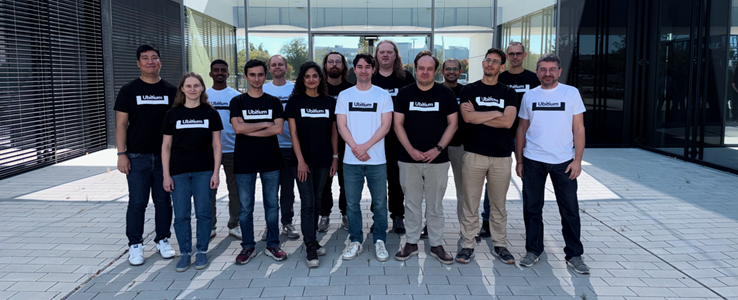
Image: Evertiq (opens in a new tab) Ubitium, a German semiconductor start up founded in 2024, has raised US$14 million in new seed funding, bringing its total seed funding to US$18 million. Ibex Investors led the round, with OpenOcean joining and existing investors KBC Focus Fund, Runa Capital and Inflection taking part again.
Florian Seibel, co founder and co chief executive of the defence technology company Quantum Systems, invested personally. Ubitium is designing one processor that handles the sensing, decision making and control tasks of an autonomous machine, with the aim of replacing the collection of specialised chips such machines typically use today.
The company plans to complete the design of its first commercial chip, the UB410, which has 4,096 processing elements, and to deliver evaluation units to customers in 2027. The round was reported by Evertiq on the basis of the company's announcement; no valuation was reported.
XIVER adds an ASML DUV stepper to its Eindhoven specialty foundryFoundry & Manufacturing · Evertiq · Summary
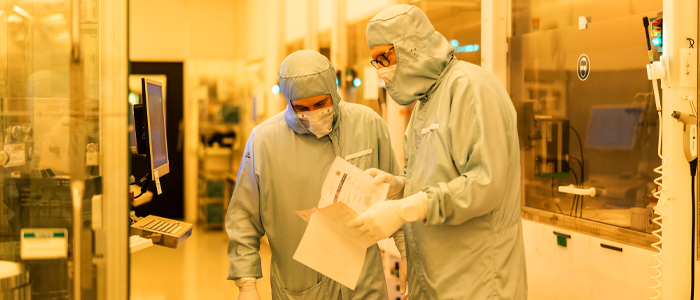
Image: Evertiq (opens in a new tab) XIVER, a Dutch specialty foundry on the High Tech Campus in Eindhoven, has bought an ASML PAS 5500 deep ultraviolet stepper to pattern finer features for photonic and semiconductor devices. The tool is expected to be running in 2027 and will work alongside the company's existing i line lithography.
XIVER says it will be the only mid sized pure play foundry with DUV lithography in house. The stepper allows finer and more precisely aligned structures, including patterning on both sides of a wafer and sub micron three dimensional micromachining.
Target products include photonic components such as waveguides and short wave infrared meta optics, as well as sensor structures built on CMOS wafers, in materials including silicon, silicon nitride, gold and thin film lithium niobate.
The chief technology officer said the tool will help photonic designs move from prototype to volume production. XIVER was spun out of Philips and bought by Dutch investors in early 2025, and has since secured €28 million in bank financing for expansion.
Former SK hynix 200mm memory fab in Eugene, Oregon, offered for saleFoundry & Manufacturing · Evertiq · Summary
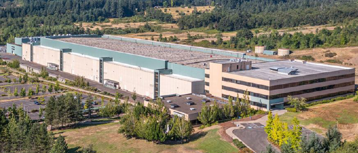
Image: Evertiq (opens in a new tab) A 200mm memory fab originally built by SK hynix in Eugene, Oregon, has been put on the market, with the semiconductor property specialist ATREG handling the sale.
The site covers about 81 hectares and includes roughly 111,500 square metres of purpose built space across three floors, of which about 15,800 square metres could serve as cleanroom production space. The largest cleanroom, about 11,150 square metres, is laid out as an open ballroom.
Cleanroom, utility and process systems are still in place, and the central utility plant was sized for 200mm production, with substantial power, water and air handling already installed. ATREG says the site is permitted and ready for a new occupant in semiconductors or a related industry, with no restrictions on title.
How much power a buyer can draw will depend on the intended use and the number of jobs created. The asking price, the current owner and how long the plant has been idle were not disclosed.
GlobalFoundries to run two Japan funded 300mm fabs in New YorkFoundry & Manufacturing · Evertiq · Summary

Image: Evertiq (opens in a new tab) GlobalFoundries has been chosen to operate two new 300mm fabs at its Malta, New York site, financed by Japan with up to US$21 billion under the trade agreement between the United States and Japan. GlobalFoundries contributes the technology and manufacturing know how.
About US$10 billion will speed construction of the first fab, which is planned to break ground later this year and come online in 2029, and a similar amount would fund the second. At full output each fab is expected to add about 900,000 wafers a year, close to the capacity of the company's whole Dresden site.
The project should create more than 1,000 skilled jobs. In separate agreements, the US government is to take an equity stake of about 4 per cent, and US$955 million of the company's existing CHIPS Act award is redirected to silicon photonics, silicon germanium and advanced packaging in New York and Vermont.
Renesas says it is planning around the new capacity.
Axcelis breaks ground on an ion implanter factory in PyeongtaekEquipment & Materials · Evertiq · Summary
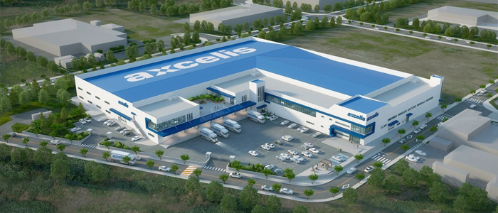
Image: Evertiq (opens in a new tab) Axcelis Technologies has started construction of a manufacturing facility for ion implantation equipment in Pyeongtaek, Gyeonggi Province, south of Seoul. The site extends the company's existing Korean base, the Axcelis Asia Operations Center.
It will have about 18,600 square metres of floor space, covering warehousing, Class 1,000 and Class 10,000 cleanrooms and a training centre. Axcelis is investing about US$35 million and plans to begin production in the second half of 2028.
When the project was first announced in September, chief executive Russell Low described ion implanters as a key front end tool and said the plant would help the company keep pace with global demand. The governor of Gyeonggi Province said the investment strengthens the region's position as a semiconductor hub.
Korea is home to two of the world's largest memory makers. The company has not said how many people the plant will employ or how much capacity it adds.
ASML reports €11.7 billion third quarter and says demand will outrun supplyEquipment & Materials · ASML (Form 6-K filed with the US SEC) · Summary
ASML reported third quarter 2026 net sales of €11.7 billion, a gross margin of 57.5 per cent and net income of €5.0 billion. The company sold 113 new and 8 used lithography systems in the quarter, and its installed base business, which covers service and upgrades, contributed €3.3 billion.
For the fourth quarter it expects net sales of €14.2 billion to €15.2 billion at a gross margin of around 57 per cent, which puts the full year at €44 billion to €45 billion with a margin of about 56 per cent.
Chief executive Christophe Fouquet said customers keep raising their short and medium term forecasts, mainly because of AI investment, and that the supply ASML has planned for 2027 and 2028 will not fully cover demand.
The company is studying how to add capacity for 2028 beyond the 30 per cent increase it announced earlier, and some customers have already asked to place orders for 2029 and 2030.
TSMC plans a further 3nm fab in Tainan for 2028Foundry & Manufacturing · Evertiq · Summary
TSMC used its investor briefing on 15 October to confirm another 3nm fab in Tainan, with production expected to begin in the first half of 2028. Chairman and chief executive C.C. Wei said he expects demand for 3nm chips to stay strong for several years.
A separate 3nm fab already under construction at the Southern Taiwan Science Park is due to start mass production in the first half of 2027, and the company is converting some 5nm capacity to 3nm to meet nearer term orders.
Outside Taiwan, the Arizona 3nm fab is ahead of plan, with tools being installed for production in the third quarter of 2027, and the second Kumamoto fab in Japan will also run 3nm from 2028.
The Tainan city government says TSMC has completed 20 fabs and packaging sites in the city and has started a 2nm fab on city owned land in Anding District. Neither the investment nor the capacity of the new fab has been disclosed.
Global chip sales pass $1 trillion for the year by August, says SIAMarkets & Policy · Semiconductor Industry Association · Summary

Image: Semiconductor Industry Association (opens in a new tab) The Semiconductor Industry Association reported worldwide semiconductor sales of US$159.7 billion for August 2026, measured as a three month moving average from World Semiconductor Trade Statistics data. That was 8 per cent more than July's US$147.9 billion and well over double the US$65.4 billion recorded in August 2025.
Cumulative sales for the year passed US$1 trillion by the end of August, a first for the industry, and the association said the market has now grown for 18 months in a row. Every region grew on the month.
On the year, the Americas rose 180.9 per cent, Asia Pacific and all other markets 143.0 per cent, China 131.3 per cent, Europe 98.5 per cent and Japan 62.3 per cent. The association now expects full year 2026 sales to exceed US$1.6 trillion, up from the US$1.5 trillion it projected in August.
Its members account for nearly all of the US industry by revenue.
Applied Materials opens its EPIC Center for shared process and equipment R&DEquipment & Materials · Evertiq · Summary

Image: Evertiq (opens in a new tab) Applied Materials unveiled its EPIC Center in Sunnyvale, California, on 12 October. The building offers about 55,700 square metres of space, including around 1.6 hectares of cleanroom, and Applied describes it as the largest facility of its kind for collaborative work on chip processes and manufacturing equipment.
The headline investment is US$5 billion, although the company says spending will build towards that figure over time as customer projects start. The idea is to put materials research, tool development and chip fabrication work under one roof so they can overlap rather than run one after another with handovers.
TSMC, Intel, Samsung, SK hynix and Micron are founding partners. Broadcom, Advantest, SCREEN, KIOXIA and Besi have joined as innovation partners, and Arizona State University, Rensselaer Polytechnic Institute, Stanford, UC Berkeley and UCLA are research partners.
Partners bring their own engineers and technical problems, and Applied expects more organisations to join.
Intel Foundry offers 300mm silicon photonics with integrated indium phosphide lasersFoundry & Manufacturing · Bits&Chips · Summary

Image: Bits&Chips (opens in a new tab) At the Open Compute Project Global Summit, Intel presented its foundry as a supplier of integrated light sources for optical links in AI data centres.
Intel says it will be the only high volume manufacturer able to build silicon photonics with indium phosphide lasers on 300mm wafers, aimed at near package and co packaged optics that bring optical connections close to processors and switches.
The process bonds indium phosphide onto a patterned silicon photonics wafer and then forms the lasers in that material, so they are aligned to the silicon waveguides by lithography instead of the careful mechanical alignment external lasers need. Intel will also support external light sources.
The company entered integrated photonics in 2016 and has so far shipped about 8 million optical transceivers and 32 million integrated lasers, which Bits&Chips describes as modest. Demand for co packaged optics from companies such as Nvidia and Broadcom is the opportunity Intel is targeting.
No mass production schedule has been announced.
Infineon extends PSOC Control C3 with post quantum secure motor and power MCUsDesign & IP · eeNews Europe · Summary

Image: eeNews Europe (opens in a new tab) Infineon has added the PSC3M/P6 series to its PSOC Control C3 microcontroller family, with the PSC3M6 aimed at motor control and the PSC3P6 at power conversion, in packages of up to 100 pins.
The devices use an Arm Cortex M33 core at up to 180 MHz and can drive up to four brushless DC motors from one chip, with or without position sensors. On chip operational amplifiers and USB and I3C interfaces reduce the need for external parts.
Target uses include industrial drives, robotics, renewable energy, power factor correction and power stages built on wide bandgap devices.
On security, the chips protect firmware in line with the US NSA's CNSA Suite 2.0 and post quantum requirements, using SHA 512 and LMS signatures to verify secure boot and updates, and support PSA Level 3 and DICE based designs. Infineon presents these features as help for makers facing the EU Cyber Resilience Act.
The parts are available now, supported by its ModusToolbox software suites.
ams OSRAM joins the Credo led OCP effort on short reach optical linksDesign & IP · eeNews Europe · Summary

Image: eeNews Europe (opens in a new tab) ams OSRAM has joined the Short Reach Micro Emitter Optics workstream within the Open Compute Project, an effort led by Credo to define interoperable standards for faster and more energy efficient optical links inside AI data centres, where growing GPU clusters are stretching what copper can do.
The approach is described as wide and slow: data is spread across many parallel channels running at moderate speed, aiming to give the reach of optics while keeping the latency, bandwidth density and cost profile of copper.
A common specification covering signalling, power efficiency, form factors, optical modules and connectors is targeted for approval by the Open Compute Project in 2027. ams OSRAM will contribute microLED and microVCSEL emitter arrays, matching photodiode receivers, CMOS technology and 3D packaging.
At ECOC 2026 it also showed an 850 nanometre thin film VCSEL platform on gallium arsenide that works with existing OM3 multimode fibre, which could lower deployment costs, and a multi core fibre connector with BizLink.
imec begins a six month evaluation of AlixLabs' pitch splitting etchEquipment & Materials · Bits&Chips · Summary
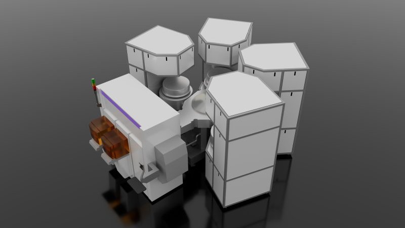
Image: Bits&Chips (opens in a new tab) AlixLabs, a Swedish equipment developer, has started a six month evaluation of its atomic layer etch pitch splitting process on imec's NanoIC pilot line in Leuven.
The technique splits a single pre patterned feature into two lines, which could double pattern density in fewer steps than conventional multiple patterning and so reduce cost and complexity at advanced nodes.
The project will test whether the process meets the dimensional and defect requirements of leading edge manufacturing. imec will first prepare and measure fine line and space patterns, AlixLabs will then tune its process on small wafer samples, and the chosen conditions will move to full wafers for imec to assess uniformity, line roughness, pitch errors and defects.
VDL Projects is supporting the engineering and build of AlixLabs' tool. AlixLabs says prospective customers asked for independent validation at imec and that it will use the results to guide process integration and equipment qualification.
No performance results have been released yet.
Gartner counts a 22.4% fall in third quarter PC shipments as memory costs biteMarkets & Policy · Electronics Weekly · Summary

Image: Electronics Weekly (opens in a new tab) Gartner estimates that about 55.4 million PCs shipped worldwide in the third quarter of 2026, 22.4 per cent fewer than the roughly 71.3 million shipped a year earlier and back to levels last seen in early 2023.
The firm puts the decline down to sharply higher memory and storage costs rather than surplus stock: it says DRAM costs roughly quintupled year on year in the second quarter, and vendors passed the increase on to buyers.
Makers also steered scarce parts towards more expensive configurations, leaving fewer low cost machines, while businesses concentrated spending on workstations and AI PCs instead of replacing whole fleets. All six leading vendors shipped fewer units.
Lenovo stayed first with about 15.0 million units and a 27.1 per cent share, down 22.4 per cent. HP fell 30.9 per cent but kept second place, Dell fell 25.4 per cent, and Apple had the smallest drop, 7.1 per cent, lifting its share to 10.5 per cent.
ASUS and Acer fell 13.0 and 11.2 per cent.
Qualcomm to begin performance based job cuts worldwide in NovemberMarkets & Policy · Electronics Weekly · Summary

Image: Electronics Weekly (opens in a new tab) Qualcomm will cut jobs across its global workforce, with notifications starting in November 2026, according to an internal memo from chief executive Cristiano Amon that was reviewed by Reuters and reported by Electronics Weekly.
The memo describes the move as a reduction focused on performance following annual reviews and says the company has repeatedly fallen short of expectations. It also argues that a broader business needs different skills and the right people in the right roles.
Qualcomm has not said how many people will be affected; it employed about 52,000 people in September 2025.
The report sets the decision against several pressures on the company: higher memory prices weighing on handset demand, MediaTek's Dimensity chips closing the gap with Snapdragon, Apple moving to its own modems faster than expected, and rising manufacturing costs squeezing margins.
Qualcomm has invested heavily in automotive, PC and data centre chips, but the report notes investors are unsure when those businesses will pay off.
Synaptics and Google launch Astra SR200 AI microcontrollers with custom DRAMDesign & IP · Electronics Weekly · Summary
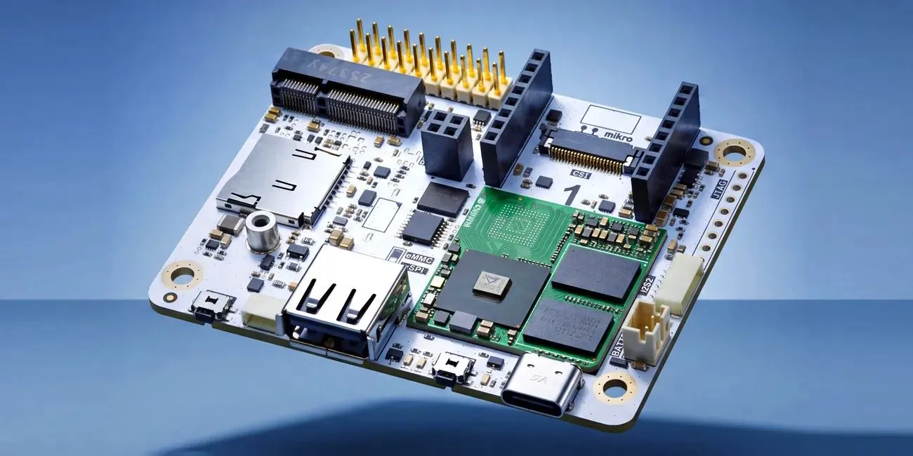
Image: Electronics Weekly (opens in a new tab) Synaptics and Google have introduced the Astra SR200 series, a family of AI microcontrollers that Synaptics calls xMCUs because they sit between conventional microcontrollers and applications processors.
Three pin compatible parts share one software kit: the SR210 at about 200 GOPS for always on voice and sensing, the SR230 at about 300 GOPS adding vision and display, and the SR250 at about 400 GOPS with dual vision and display paths.
Up to 8MB of on chip SRAM is paired with custom DRAM that can scale to hundreds of megabytes, which the companies say runs at roughly a third of the power of typical system memory. The Torq AI engine integrates Google's Coral NPU and uses an open source MLIR and IREE compiler.
Compute comes from Arm Cortex M85 and Cortex M52 cores, with an optional Cadence Tensilica HiFi 5 DSP for audio. The security engine targets PSA Level 3 and Common Criteria EAL4+.
Pricing and sample dates were not given.
Jury finds Arm breached its licence with Qualcomm but awards $2 in damagesDesign & IP · Electronics Weekly · Summary

Image: Electronics Weekly (opens in a new tab) A US jury has found that Arm breached its architecture licence agreement with Qualcomm by withholding chip testing tools and software patches, and that Arm deliberately tried to disrupt Qualcomm's business by leaking a letter about revoking Qualcomm's licence.
Qualcomm had argued that the leak cost it a deal with Meta worth about US$170 million. Of Qualcomm's six claims, Arm won four and Qualcomm two, and Qualcomm was awarded nominal damages of US$1 for each claim it won, US$2 in total, after Arm argued there was no direct, measurable loss.
Both companies presented the outcome as favourable: Arm pointed to the claims it won and the token award, while Qualcomm stressed the breach finding.
The judge still has to rule on whether Arm negotiated in good faith over licensing its v10 technology, and on whether Qualcomm can use a contract clause to stop paying Arm royalties for five years, a sum reported at more than US$2 billion.
Memory makers reportedly to build Nvidia custom HBM base dies on TSMC 3nmPackaging & Test · Electronics Weekly · Summary
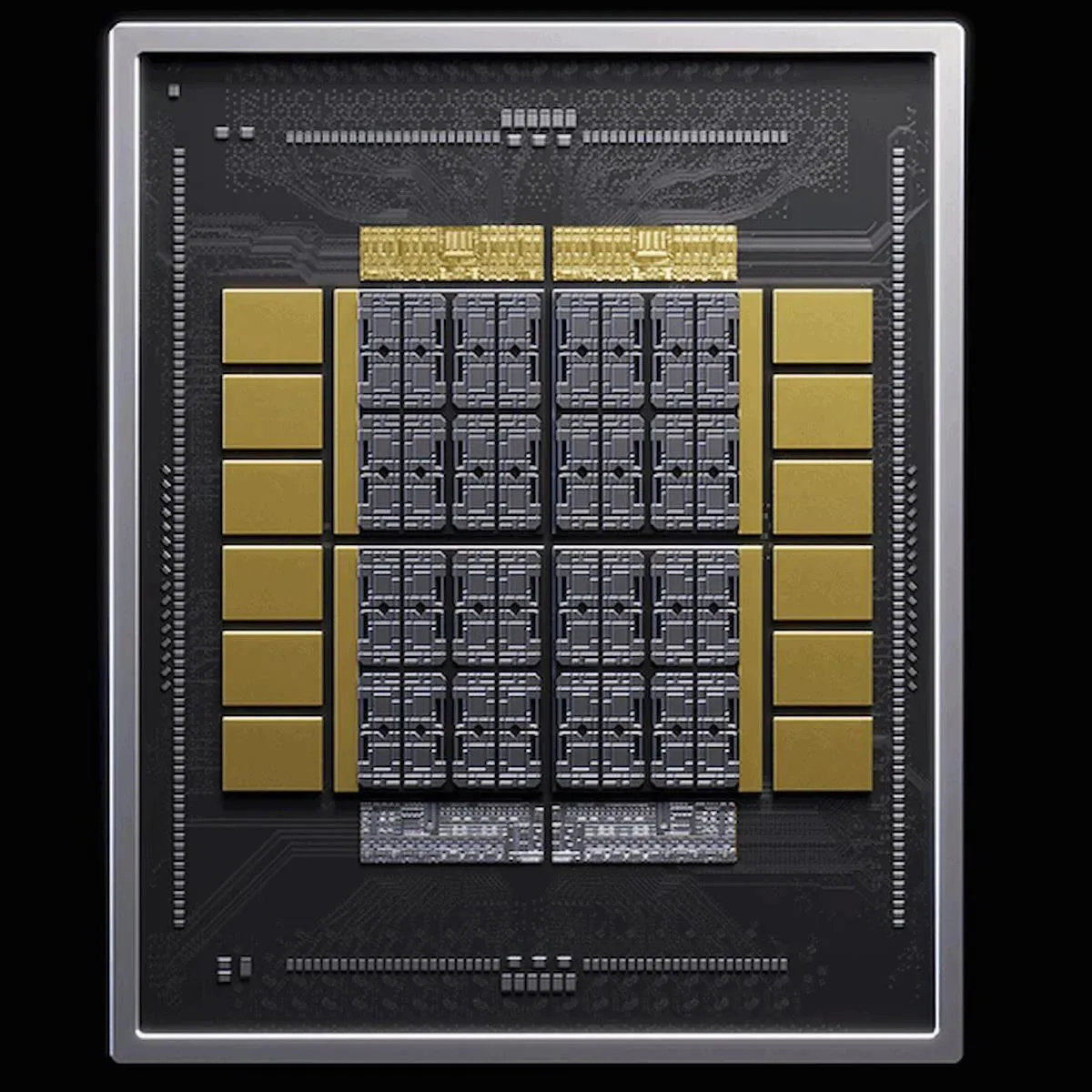
Image: Electronics Weekly (opens in a new tab) Nvidia has asked Samsung, SK hynix and Micron to make the base dies for its custom high bandwidth memory, known as NVHBM, on TSMC's 3nm process, according to a report in the Seoul Economic Daily summarised by Electronics Weekly.
The base die is the logic layer at the bottom of an HBM stack that handles the interface and, in this design, a memory controller moved off the GPU. Nvidia wants a single base die design and process across its suppliers so it does not have to validate a different version from each one.
Samsung and Micron are reported to have agreed; SK hynix already uses TSMC's 12nm process for its HBM4 base dies. Nvidia claims NVHBM offers up to 30 per cent more bandwidth and 15 per cent lower power than standard HBM4E, with volume production expected in 2027.
Samsung is also said to be qualifying base dies on its own 2nm process as a fallback and will keep making standard HBM for other customers.
EDA and IP revenue grew 12.2% in the second quarter, ESD Alliance reportsEDA & Tools · Electronics Weekly · Summary
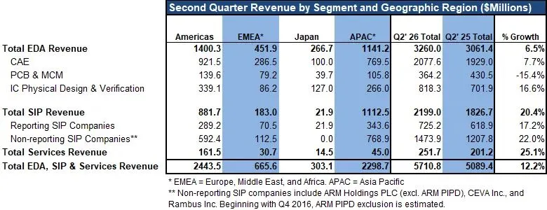
Image: Electronics Weekly (opens in a new tab) The ESD Alliance, part of SEMI, reports that electronic system design revenue rose 12.2 per cent year on year to US$5,710.8 million in the second quarter of 2026, from US$5,089.4 million a year earlier. Semiconductor IP was the largest and one of the fastest growing categories at US$2,199.0 million, up 20.4 per cent.
Computer aided engineering grew 7.7 per cent to US$2,077.6 million, IC physical design and verification 16.6 per cent to US$818.3 million and services 25.1 per cent to US$251.7 million, while PCB and multi chip module tools fell 15.4 per cent to US$364.2 million.
Every region grew: the Americas by 7.1 per cent to US$2,443.5 million, Asia Pacific by 22.4 per cent to US$2,298.7 million, EMEA by 2.3 per cent and Japan by 9.3 per cent. Headcount at the tracked companies fell 1.6 per cent to 71,396.
Walden Rhines, executive sponsor of the report, noted that only the PCB and MCM category declined.