News from October 2026
665 stories of semiconductor news published on the Hub in October 2026, newest first and grouped by day (UTC). Each headline opens the story's page on the Hub, with a summary and a link to the original report.
Showing 401 to 450 of 665 stories.
Monday 26 October 202679 stories
Streamlined Development Platforms Are Now Critical to Edge AI DeploymentMarkets & Policy · Embedded.com · Summary
Streamlining development platforms has become a trend in the embedded industry, as the demand for deploying larger AI and machine-learning (ML) models at the edge increases development complexity, time, and, thereby, cost.
The architectural diversity of embedded edge devices means that models must be converted, quantized or otherwise optimized, compiled for the target runtime, and [...] The post Streamlined Development Platforms Are Now Critical to Edge AI Deployment appeared first on Embedded.
Silicon Carbide and Gallium Nitride Play Growing Role in Electronics Design, Manufacturing and Supply-Chain StrategyEquipment & Materials · Global Electronics Association (formerly IPC) · Summary

Image: Global Electronics Association (formerly IPC) (opens in a new tab) Silicon Carbide and Gallium Nitride Play Growing Role in Electronics Design, Manufacturing and Supply-Chain Strategy 431279_sandyge… Oct 26, 2026 Oct 26, 2026 New research from the Global Electronics Association and Accuris launches a series examining technology trends shaping the electronics industry Silicon carbide (SiC) and gallium nitride (GaN) power devices are expanding their role in electronics, with implications extending beyond component selection to product design, manufacturing capab…
The AI Packaging Challenge: 5 Reasons Panels Are Gaining MomentumPackaging & Test · EE Times · Summary

Image: EE Times (opens in a new tab) As AI pushes chip packages beyond traditional wafer limits, panel-level processing is emerging as a critical path to scale advanced packaging. The post The AI Packaging Challenge: 5 Reasons Panels Are Gaining Momentum appeared first on EE Times.
Former Intel CEO Pat Gelsinger bets on Nagare Labs to vault the memory wallMarkets & Policy · The Register · Summary
Image: The Register (opens in a new tab) SRAM-like bandwidth, DRAM-like density, and NAND-like manufacturing: Z2RAM makes big promises, but the road ahead is arduous and littered with the ruins of failed memory vendors
Nvidia RTX 20, 30, and 40-series GPUs hacked to remove a half-speed AI throttleDesign & IP · Tom's Hardware · Summary

Image: Tom's Hardware (opens in a new tab) Linux kernel modules lift Nvidia’s half-rate AI tensor limit on GeForce RTX 20, 30, and 40-series GPUs.
Modder turns NES into a Windows-like desktop with original hardwareDesign & IP · Tom's Hardware · Summary
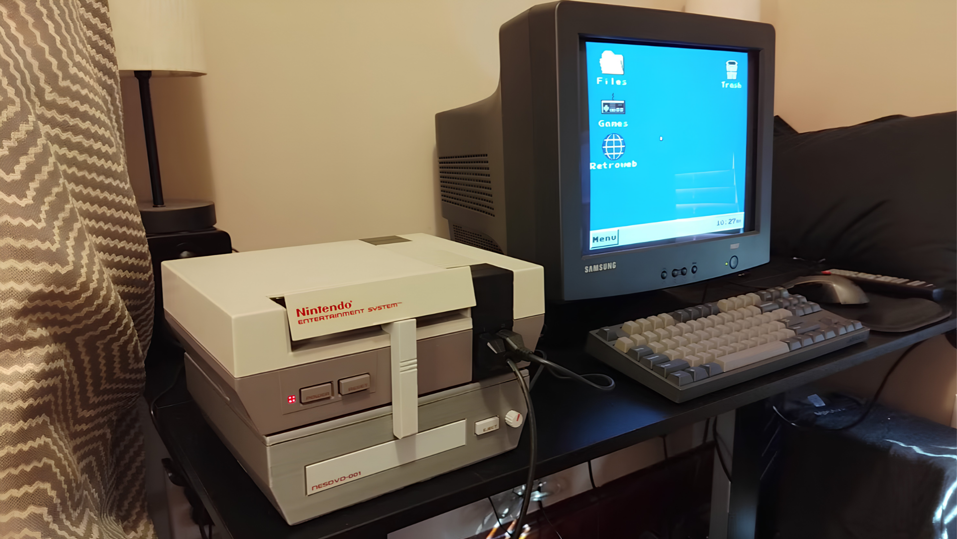
Image: Tom's Hardware (opens in a new tab) Throaty Mumbo turns his NES into a Windows-like desktop using an FPGA cartridge emulating an old Intel CPU, complete with a CD drive and internet capabilities, all without tearing the NES apart.
Electronics production growth accelerates on AI demandMarkets & Policy · eeNews Europe · Summary

Image: eeNews Europe (opens in a new tab) Electronics production growth accelerated across major manufacturing economies in 2026, with demand for AI infrastructure driving particularly rapid expansion in Taiwan, according to an analysis published on 22 October by Semiconductor Intelligence.
The expansion contrasts with falling PC and smartphone shipments as the AI boom puts pressure on memory supply and pricing. Electronics production growth […] The post Electronics production growth accelerates on AI demand appeared first on eeNews Eu…
Meta announces $95 billion stock offering to fund AI expansionMarkets & Policy · CNBC Technology · Summary

Image: CNBC Technology (opens in a new tab) Meta said Monday it is planning to raise a total of $95 billion to support itsi nvestments in AI infrastructure and super intelligence.
Weekly Radar 007: NVIDIA Moves to Secure Substrate CapacityEquipment & Materials · TrendForce Insights · Summary
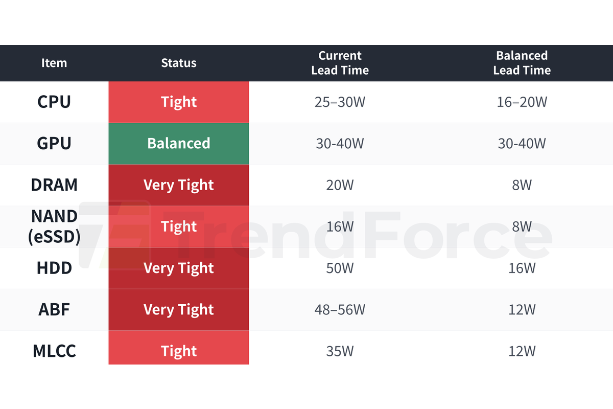
Image: TrendForce Insights (opens in a new tab) ABF stays Very Tight with little near-term relief.
CScale exits Stealth with $145m funding for gigawatt-scale AIMarkets & Policy · Electronics Weekly · Summary
CScale, a Palo Alto startup for optical interconnects, has exited stealth mode with the announcement of $145 million in Series C funding. Nvidia and Intel Capital were among the investors. […] The post CScale exits Stealth with $145m funding for gigawatt-scale AI appeared first on Electronics Weekly.
Palomino gains first commercial purchase order from strategic hyperscaler customerEquipment & Materials · Semiconductor Today · Summary
Artificial intelligence (AI) interconnect technology company Palomino Laboratories Inc of Goleta, CA, USA has received its first purchase order (PO) from a strategic hyperscaler customer.
The PO includes a statement of work (SOW) for the delivery of high-performance gallium nitride (GaN) micro-LED chips for optical interconnect applications within AI infrastructure...
University of Illinois at Urbana-Champaign (UIUC) has achieved a record modulation bandwidth of 2.75GHz in a gallium nitride (GaN) blue micro-LED (Abdelghany Abouelnagga et aEquipment & Materials · Semiconductor Today · Summary
University of Illinois at Urbana-Champaign (UIUC) has achieved a record modulation bandwidth of 2.75GHz in a gallium nitride (GaN) blue micro-LED (Abdelghany Abouelnagga et al...
Rapidus and HCLTech announce partnership for next-generation semiconductor technologiesFoundry & Manufacturing · PR Newswire · Summary
TOKYO and NOIDA, India, Oct. 26, 2026 /PRNewswire/ -- HCLTech (NSE: HCLTECH) (BSE: HCLTECH), a leading global technology company, and Rapidus Corporation, a Japanese company developing and manufacturing advanced logic semiconductors, today officially inaugurated two HCLTech development...
Neocloud stocks fall as Elon Musk says more than 200 of them face 'guppy-level death'Markets & Policy · CNBC Technology · Summary

Image: CNBC Technology (opens in a new tab) Investors are already questioning the debt-fueled expansion of neoclouds and whether the large AI infrastructure build-out will generate long-term returns.
Reliable HCI-based programming in V-NAND flash memory: co-optimization of SWL waveform and trap-cut architectureDesign & IP · Semiconductor Science and Technology (IOP) · Summary
Hot carrier injection-based programming has emerged as a high-efficiency alternative to conventional Fowler–Nordheim (FN) tunneling for next-generation vertical NAND (V-NAND), yet its practical implementation is severely constrained by coupled physical reliability trade-offs: program disturb, Z-interference, and retention degradation.
This study investigates these bottlenecks through technology computer-aided design simulations calibrated to experimental PN junction and V-NAND reference data, a…
How do you characterize temp sensor chip in mass production?Foundry & Manufacturing · r/chipdesign · Summary
I'm wondering how the temperature sensor chip would characterize/trim the temperature coefficient of the system for mass production. Can you do two temperature point measurement for all of the chip at package level?
Or you do it at wafer level? Do you measure every die/package or just one chip to represent the whole lot.
From what I understand, it takes time to heat up the environment, so doing two point measurement for every package is expensive. Not sure how it is done for temperature sensor …
Compact analytical–numerical drift-region design rules for quasi-vertical GaN trench MOSFETsEquipment & Materials · Semiconductor Science and Technology (IOP) · Summary
A compact analytical–numerical framework is developed for drift-region design in quasi-vertical gallium nitride (GaN) trench metal–oxide–semiconductor field-effect transistors. The forward model combines finite-thickness electrostatics, an equivalent fixed-charge correction, GaN avalanche ionization, and trench-to-drift current spreading.
Four fixed-thickness structures first verify the field regime, breakdown voltage, and specific on-resistance against two-dimensional technology computer-aided…
Server CPUs to grow 30% in 2026 and 40% in 2027Design & IP · Electronics Weekly · Summary
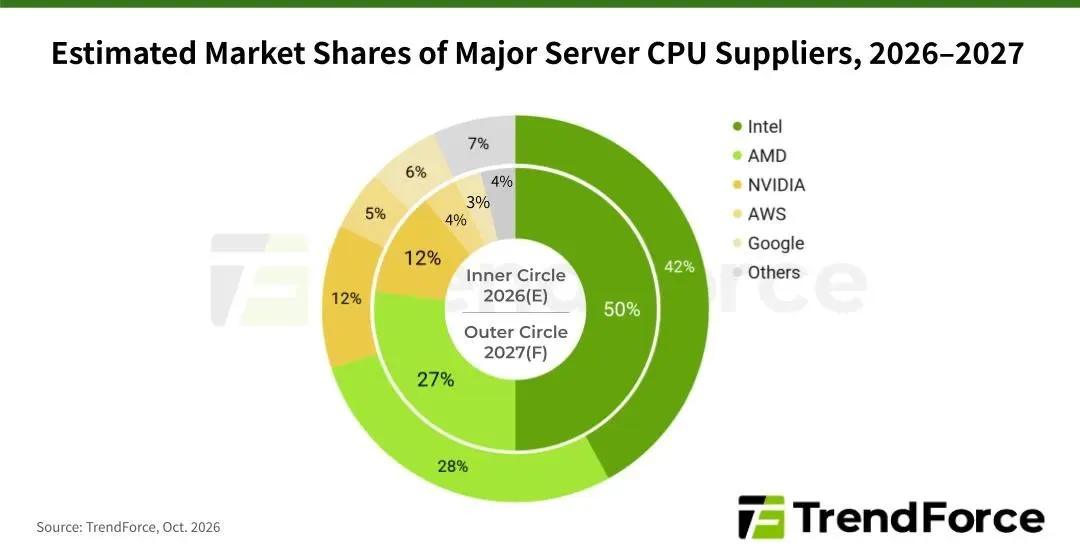
Image: Electronics Weekly (opens in a new tab) Server CPU shipments are projected to increase 31% YoY in 2026. In 2027, continued growth in AI inference demand and rising adoption of agentic AI services are expected to drive […] The post Server CPUs to grow 30% in 2026 and 40% in 2027 appeared first on Electronics Weekly.
Atomera and IQE hook up to advance RF GaNEquipment & Materials · Electronics Weekly · Summary
Image: Electronics Weekly (opens in a new tab) Atomera, a semiconductor transistor materials and technology licensing company, has entered into a Joint Development Agreement (JDA) with IQE to bring high-performance, cost-effective RF GaN to market. The collaboration leverages […] The post Atomera and IQE hook up to advance RF GaN appeared first on Electronics Weekly.
Self-Heating And Parasitics Challenge Multi-Tier CFET Scaling (TU Munich, IIT Kanpur)Foundry & Manufacturing · Semiconductor Engineering · Summary
Researchers at the Technical University of Munich and Indian Institute of Technology Kanpur published “Self-Heating and Parasitic Effects in Multi-Tier CFET Design.”
Abstract Excerpt: “We study the impact of self-heating effects (SHEs) and middle of line (MOL) and back-end of line (BEOL) induced parasitics on multi-tier CFET design, where multiple nanosheet devices are vertically stacked.... » read more The post Self-Heating And Parasitics Challenge Multi-Tier CFET Scaling (TU Munich, IIT Kanpu…
Bringing Down Test Costs For Co-Packaged OpticsPackaging & Test · Semiconductor Engineering · Summary

Image: Semiconductor Engineering (opens in a new tab) Pinpointing failures, ensuring known-good optical engines, and controlling test costs become increasingly critical as photonics moves into advanced packages. The post Bringing Down Test Costs For Co-Packaged Optics appeared first on Semiconductor Engineering.
Testing Silicon Photonics At ScalePackaging & Test · Semiconductor Engineering · Summary

Image: Semiconductor Engineering (opens in a new tab) New test requirements include fiber alignment, coupling efficiency, polarization management, and optical instrumentation. The post Testing Silicon Photonics At Scale appeared first on Semiconductor Engineering.
Large-Format Masks Move From Aspiration To Industry RoadmapMarkets & Policy · Semiconductor Engineering · Summary

Image: Semiconductor Engineering (opens in a new tab) Expert panel sees a compelling productivity case, but the entire photomask ecosystem must be ready together. The post Large-Format Masks Move From Aspiration To Industry Roadmap appeared first on Semiconductor Engineering.
Vertical DRAM Stacking Expands Thermal Design Space Beyond HBM-on-GPU (imec)Packaging & Test · Semiconductor Engineering · Summary

Image: Semiconductor Engineering (opens in a new tab) Researchers at imec published “Beyond HBM-on-GPU: Thermal Design Envelope for 3D Volumetric DRAM-on-GPU Integration.” Summary: Researchers evaluated a 3D memory architecture that rotates DRAM dies vertically above a GPU and places cooling cavities between them as an alternative to conventional 2.5D HBM and direct-stacked HBM-on-GPU.
Package-level thermal simulations examined stack height, memory capacity and organization,... » read more The post Vertical DRAM Stacking Expands Thermal Design Spa…
South Korea urged to guard chip profitability as China’s CXMT and YMTC gain market sharePackaging & Test · South China Morning Post - Tech · Summary
China’s expanding semiconductor industry is fuelling mounting anxiety in South Korea, where a new consultancy report has warned local chipmakers to defend profitability as Chinese rivals scale up production and strengthen market share.
Samil PwC, the South Korean member firm of the global consultancy, said in a report made public on Monday that Chinese competition would likely heat up first in the areas of conventional memory, mature-node manufacturing, and packaging and testing. To stay ahead,…
MERA: A Mid-Circuit-Measurement Error-Aware Compilation Framework for Quantum CircuitsDesign & IP · arXiv cs.AR (Hardware Architecture) · Summary
Mid-circuit measurement (MCM) enables qubit reuse and dynamic control in quantum processors, underpinning resource-efficient algorithms and quantum error correction. However, MCM introduces non-negligible errors, including measurement-induced crosstalk, idling-qubit decoherence, and reset infidelity.
Additionally, MCM error rates vary across qubits within the same processor, with some exhibiting substantially higher errors. Existing compilers, including Qiskit-compiler and QR-Map, ignore MCM er…
Toward Open ISA Supercomputing: A Comparative Study of RISC-V, Arm, and x86 Architectures on HPC WorkloadsDesign & IP · arXiv cs.AR (Hardware Architecture) · Summary
RISC-V is emerging as a candidate architecture for high-performance computing (HPC), but its competitiveness against established x86 and Arm processors remains difficult to assess because existing studies use different platforms, workloads, and methodologies, and rarely consider energy efficiency.
Our work provides an evaluation of contemporary HPC RISC-V, Arm, and x86 processors using a common software stack and methodology. We characterize the Sophgo SG2044 and compare it with the NVIDIA Grac…
A Resource-Efficient and Precision-Scalable FPGA Accelerator for Spiking Neural Networks Using Minifloat ArithmeticDesign & IP · arXiv cs.AR (Hardware Architecture) · Summary
Spiking neural networks (SNNs) are well suited to event-driven edge intelligence, but the arithmetic complexity, memory footprint, and power consumption associated with conventional floating-point implementations can limit their deployment on resource-constrained hardware.
This paper presents a precision-scalable and resource-efficient SNN hardware accelerator architecture based on parameterized minifloat arithmetic. The proposed architecture implements recurrent leaky integrate-and-fire (LIF) …
Decode Late, Multiply Once: Rethinking the Dot Product for Quantized WeightsMarkets & Policy · arXiv cs.AR (Hardware Architecture) · Summary
Large neural networks are increasingly deployed with 1-4 bit weights and 16- or 32-bit activations, yet their dot products still use one multiplier per element. We show that a length-n dot product with k-bit weight codes can be computed with n+2^k additions and at most 2^k decodes and 2^k multiplications.
Each weight code is used directly as an address offset that selects one of 2^k accumulators; each activation is added into the selected accumulator; and the accumulated sums are decoded and mu…
Embodied Emissions of 2.5D and 3D Scaling in Chipletized GPUs for Low-Carbon AIPackaging & Test · arXiv cs.AR (Hardware Architecture) · Summary
GPU compute resources are scaling to support growing AI workloads, leading to further rises in the climate change impact of hyperscale data centers that rely on high-performance GPUs.
To model how packaging decisions impact the carbon footprint we have estimated the embodied emissions (EE) of a chiplet-based GPU that has been scaled in 2.5D and 3D using the imec.netzero modelling platform. We doubled the number of compute units and high bandwidth memory (HBM) capacity in the 2.5D and 3D scaled …
Automated Multi-Line Bug Repair Using Model Checker Aided LLMs: A Case Study on RISC-V ProcessorsDesign & IP · arXiv cs.AR (Hardware Architecture) · Summary
Functional verification of Register-Transfer Level(RTL) designs has become a critical bottleneck in modern semiconductor development, often consuming the majority of project resources. Debugging, in particular, remains an especially time-consuming task, requiring careful analysis of simulation traces or counterexamples.
Recent work has explored applying Large Language Models (LLMs) to RTL debug and repair with great promise. However, the existing approaches typically are for single-line bugs, o…
TranSAGE: Automating Spatial Accelerator Generation for Large-Scale Transformer ModelsDesign & IP · arXiv cs.AR (Hardware Architecture) · Summary
Large-scale Transformers have achieved remarkable success across NLP, computer vision, and robotics, but their growing computational and memory demands challenge efficient inference. Spatial accelerators offer advantages in on-chip bandwidth and energy efficiency, yet designing them for large models remains costly and time-consuming.
Existing accelerator generators typically focus on single-operation support, overlooking the benefits of multi-operation pipelining, which limits throughput and en…
Chips and Cheese: ""Performance" Oryon: Qualcomm's Little Core"Markets & Policy · r/hardware · Summary

Image: r/hardware (opens in a new tab) submitted by /u/Dakhil [link] [comments]
System Check: What is next for industrial RF engineering?Design & IP · eeNews Europe · Summary

Image: eeNews Europe (opens in a new tab) Ready for the next System Check! Industrial RF design powers automation, wireless communications, and connected systems.
We want to know which technologies you think will shape its future. Where will AI have the greatest impact?
Past results We recently asked our community members about FPGAs and whether they work with them. Let’s consider the results. […] The post System Check: What is next for industrial RF engineering? appeared first on eeNews Europe.
SpaceX closes $40 billion debt deal for AI chips, Elon Musk saysDesign & IP · CNBC Technology · Summary
Elon Musk said in an X post that SpaceX has closed $40 billion in debt financing to purchase GPUs.
Leaked footage shows Chinese factories converting hundreds of RTX 5090s into dual-slot GPUs for AI servers, using their GB202 chips and GDDR7 memoryDesign & IP · r/hardware · Summary

Image: r/hardware (opens in a new tab) submitted by /u/sr_local [link] [comments]

Sunday 25 October 202645 stories
Aivres NVIDIA Vera Rubin and HGX B300 at OCP SummitMarkets & Policy · ServeTheHome · Summary
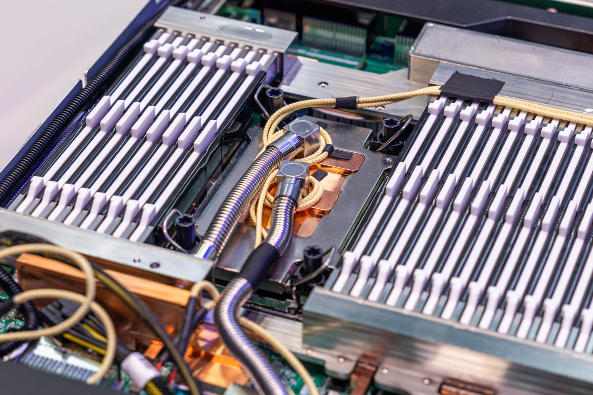
Image: ServeTheHome (opens in a new tab) We check out the range of Aivres NVIDIA Vera, Vera Rubin, and Blackwell Ultra platforms at OCP Summit 2026 The post Aivres NVIDIA Vera Rubin and HGX B300 at OCP Summit appeared first on ServeTheHome.
Dry-Deposited Resist Shows Different Tone Behavior Under EUV And E-Beam Exposure (KU Leuven, Kunsan, VUB, Imec)Equipment & Materials · Semiconductor Engineering · Summary

Image: Semiconductor Engineering (opens in a new tab) Researchers at KU Leuven, Kunsan National University, Vrije Universiteit Brussel, imec, et al. published “Irradiation-Source-Dependent Tone Conversion in Dry-Deposited Halogenated Amorphous Zeolitic Imidazolate Framework Resists for Electron-Beam and Extreme Ultraviolet Lithography.”
Abstract Excerpt: “Dry-deposited metal–organic resists are key enablers for advanced patterning processes in next-generation semiconductor manufacturing. Here, we report halogenated amorphous zeolitic imidazolate f…
Pt-W Alloy Shows Potential For Thinner High-NA EUV Mask Absorbers (Chinese Academy of Sciences et al.)Equipment & Materials · Semiconductor Engineering · Summary

Image: Semiconductor Engineering (opens in a new tab) Researchers at Chinese Academy of Sciences, Jilin University, State Key Laboratory of Advanced Manufacturing for Optical Systems, and University of Chinese Academy of Sciences published a technical paper titled “Evaluating an alternative Pt-W alloy as a low-n EUV mask absorber: Film properties and imaging performance.”
“In this study, we investigate an alternative Pt-W alloy as... » read more The post Pt-W Alloy Shows Potential For Thinner High-NA EUV Mask Absorbers (Chinese Academy of Sciences…
Neural Networks Speed 3nm Nanosheet SPICE Simulation (TU Munich)Foundry & Manufacturing · Semiconductor Engineering · Summary

Image: Semiconductor Engineering (opens in a new tab) Researchers at Technical University of Munich published “NN-Based Transistor Modeling for Ultra-Fast SPICE Simulation and Standard Cell Library Characterization.” Abstract: “Neural network (NN)-based transistor models have proven to be a promising solution to accelerate device modeling.
Although these models demonstrated remarkable speedup in circuit simulations, they were not rigorously tested in complex tasks within standard... » read more The post Neural Networks Speed 3nm Nanosheet SPICE Si…
Security-Aware Layer Mapping Reduces Fault Vulnerability In 3D Compute-In-Memory (ASU, U. of Maryland)Design & IP · Semiconductor Engineering · Summary

Image: Semiconductor Engineering (opens in a new tab) Researchers at Arizona State University and University of Maryland published “SEAL: Multitenant Security-Aware Layer Mapping for Heterogeneous 3-D CiM Accelerators.”
Abstract: “Heterogeneous 3-D compute-in-memory architectures can combine different memory technologies across stacked tiers to accelerate deep neural network inference, but multitenant deployments introduce security risks through shared power delivery networks. The researchers developed SEAL, a security-aware... » read more The pos…
Silicon Photonic Modulator Reaches 200 Gb/s PAM4 With Reduced DSP (Science Tokyo, Yokohama, AIST, PETRA)Markets & Policy · Semiconductor Engineering · Summary

Image: Semiconductor Engineering (opens in a new tab) Researchers from Institute of Science Tokyo, Yokohama National University, AIST, and Photonics Electronics Technology Research Association (PETRA) published a technical paper titled “Reduced-DSP 200G/λ Low-Voltage Slow-Light Silicon Modulator Enabled by Built-In EO Equalizer.”
Abstract Excerpt: “Multi-Tb/s optical interconnects for artificial intelligence data centers necessitate high-speed, energy-efficient, and compact transceivers. However, conventional silicon Mach-Zehnder modulators are...…
Which are the top VLSI companies in Bangalore? (Product vs Service vs EDA breakdown)EDA & Tools · r/semiconductors · Summary
submitted by /u/Puzzleheaded-Gas8907 [link] [comments]
Solidigm pulled its IPO and neocloud credit spreads are blowing out ahead of hyperscaler earningsPackaging & Test · r/semiconductors · Summary
Solidigm scrapped its IPO this week, and credit default swap spreads across neocloud companies have been widening while their stocks fall. The timing puts the AI buildout's funding under its first real stress test just days before the biggest hyperscalers report.
Nvidia has moved beyond selling chips into effectively financing parts of the AI buildout, which puts an unusual amount of balance-sheet weight on one company. If neocloud borrowing costs keep climbing and new equity raises stay shut, …
EU-US-China geopoliticsMarkets & Policy · r/semiconductors · Summary
Hello! I have a question regarding the impact of the US–China chip war on the EU's strategic autonomy.
I'm reaching out because I haven't been able to find anyone at my university who could help me understand the geopolitics behind this issue, and I would really appreciate some guidance. Is there a connection between the US–China chip war and the EU?
Does this conflict affect the EU's strategic autonomy in any way? So far, I've been considering analyzing, from a neorealist perspective, how the …
Hygon's first nine months showed 58% revenue growth year over year and a swing to net operating cash outflowMarkets & Policy · r/semiconductors · Summary
Operating cash flow turned negative in Hygon Information Technology's first nine months of the year, reversing an inflow over the same period a year earlier. I subtracted the half-year figure from the nine-month total, and about 2 billion yuan of that outflow fell in the third quarter.
Third quarter revenue was up 45% from a year earlier and net income attributable to shareholders grew 38%. Those are not the numbers of a company in decline.
Hygon's unaudited filing says it increased inventory t…
Exploring semiconductor industry and India's progressMarkets & Policy · r/semiconductors · Summary
submitted by /u/CHEEMz05 [link] [comments]
Semiconductor workers: Any worries about the recent stock market crashes?Markets & Policy · r/semiconductors · Summary
I'm working at a semiconductor OEM. Every signal entering my brain suggests that the industry is booming and will continue to, yet the recent selloffs have been insane.
I haven't been in the industry long enough to know how this will affect it. Any veterans in the field mind sharing how your work environment have been affected by the ups and downs of the market? submitted by /u/JamesBummed [link] [comments]
Just bought a full pallet of sealed Okmetic 6" prime wafers – any advice on selling them in Europe?Equipment & Materials · r/semiconductors · Summary
Hi all, I just bought a full pallet of silicon wafers at a bankruptcy auction here in Finland. They're unopened Okmetic boxes: 1,600 pcs of 6" (150 mm) prime grade wafers.
I'm not in the semiconductor industry, so I'm looking for advice: Is it realistic for a private individual to sell these in Europe? Who would typically buy wafers like this: labs, universities, small fabs, MEMS startups, resellers?
Any tips on pricing or where to list them? Thanks! submitted by /u/Alarming-Singer762 [link] [c…
CEO Interview with Eric Tsai of MiviumEquipment & Materials · SemiWiki Forums · Summary

Image: SemiWiki Forums (opens in a new tab) Eric Tsai is Co-Founder and CEO of Mivium, Inc., a US-based materials technology company in Fremont, California developing submicron gallium nitride powder and related wide bandgap materials.
He co-founded Mivium in 2022 after a career building and scaling consumer businesses, most recently as Vice President of Marketing… Read More The post CEO Interview with Eric Tsai of Mivium appeared first on SemiWiki.