Term · Reliability & Quality
Electromigration
Gradual transport of metal atoms along an interconnect caused by momentum transfer from the electron current, producing voids that open the line and hillocks that short to neighbours.
It sets the maximum sustained current density allowed per wire and via.
- Also known as
- EM
- Type
- Term
- Domain
- Reliability & Quality, Failure mechanisms
- Also relevant to
- Process Technology
Notes
The dominant back end of line wear-out limit; the industry moved from aluminium to copper largely to buy electromigration margin.
Overview
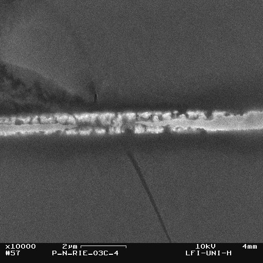
Electromigration is the gradual transport of metal atoms along a conductor, driven by the momentum of the electrons flowing through it, which over time creates voids that break wires and hillocks that can short them to their neighbours. It is one of the main wear-out mechanisms in chip interconnect, and it sets how much current each wire and via may carry over a product's lifetime.
How it works
In a wire carrying current, electrons collide with metal atoms and push them, on average, in the direction of electron flow. At normal current densities the effect is negligible, but in the narrow wires of modern chips densities are high, and over years atoms pile up downstream and leave gaps upstream. Atoms move most easily along grain boundaries and interfaces, which is why capping layers on copper lines matter.
Lifetime falls steeply as current density and temperature rise. Engineers use empirical models, most famously Black's equation from the late 1960s, which relate median time to failure to current density and an activation energy, and run accelerated tests at high current and temperature to measure the parameters for each metal layer and via. AEC-Q100 lists electromigration among its die fabrication reliability tests for automotive qualification.
The results become design rules: maximum current per unit width for each layer, adjusted for temperature and lifetime target. Short wires can benefit from a back-stress effect that resists migration. As wires shrink, and in advanced packages where solder bumps and redistribution layers carry high currents, electromigration remains an active reliability concern.
Related terms
Part of the Reliability & Quality glossary, with every term in the topic and the lifecycles, tools and standards that use them.
Where it appears on the Hub
Used on 42 pages of the Hub. In each group, the pages that mention it most come first.
Lifecycle stages and gates
- Extraction correlated to silicon (PDK lifecycle)
- Parasitic Extraction & Technology Files (PDK lifecycle)
- Physical Sign-off & Characterisation (Hard IP lifecycle)
- Post-layout sign-off (AMS lifecycle)
- Post-Layout Verification & Sign-off (AMS lifecycle)
- Design and layout freeze (Hard IP lifecycle)
- and 9 more
Suggest an improvement
Suggest an improvement to this entry
A clearer definition, an example, a correction or a source an editor can check. Editors review every suggestion before the entry changes.
Last reviewed . Written by The Semiconductor Hub editorial team. The full glossary