News / Equipment & Materials / Piezo-Driven Active Wafer Shaping Improves Precision in Semicon Manufacturing
Piezo-Driven Active Wafer Shaping Improves Precision in Semicon Manufacturing
By The Semiconductor Hub news desk ·
Link post
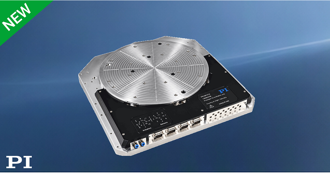
Programmable active wafer chuck corrects bow, warpage and localized surface deviations on substrates up to 300 mm SAN FRANCISCO, Nov. 10, 2026 /PRNewswire/ -- As semiconductor processes place increasingly stringent demands on wafer flatness and positioning, PI (Physik Instrumente) has...
Read at PR NewswireSource: PR Newswire, published . The summary is the Hub's own; the full story is at the source. Report a rights or accuracy concern